
A new way of making large sheets of high-quality, atomically thin graphene could lead to ultra-lightweight, flexible solar cells, and to new classes of light-emitting devices and other thin-film electronics.
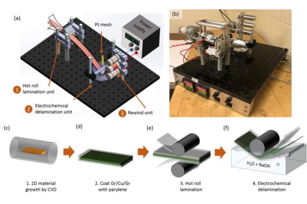
The new manufacturing process, which was developed at MIT and should be relatively easy to scale up for industrial production, involves an intermediate “buffer” layer of material that is key to the technique’s success. The buffer allows the ultrathin graphene sheet, less than a nanometer (billionth of a meter) thick, to be easily lifted off from its substrate, allowing for rapid roll-to-roll manufacturing.
This process is detailed in a paper published in Advanced Functional Materials, by MIT postdocs Giovanni Azzellino and Mahdi Tavakoli; professors Jing Kong, Tomas Palacios, and Markus Buehler; and five others at MIT.
The state-of-the-art
Finding a way to make thin, large-area, transparent electrodes that are stable in open air has been a major quest in thin-film electronics in recent years, for a variety of applications in optoelectronic devices — things that either emit light, like computer and smartphone screens, or harvest it, like solar cells. Today’s standard for such applications is indium tin oxide (ITO), a material based on rare and expensive chemical elements.
Many research groups have worked on finding a replacement for ITO, focusing on both organic and inorganic candidate materials. Graphene, a form of pure carbon whose atoms are arranged in a flat hexagonal array, has extremely good electrical and mechanical properties, yet it is vanishingly thin, physically flexible, and made from an abundant, inexpensive material. Furthermore, it can be easily grown in the form of large sheets by chemical vapor deposition (CVD), using copper as a seed layer, as Kong’s group has demonstrated. However, for device applications, the trickiest part has been finding ways to release the CVD-grown graphene from its native copper substrate.
The new process
This release, known as graphene transfer process, tends to result in a web of tears, wrinkles, and defects in the sheets, which disrupts the film continuity and therefore drastically reduces their electrical conductivity. But with the new technology, Azzellino says, “now we are able to reliably manufacture large-area graphene sheets, transfer them onto whatever substrate we want, and the way we transfer them does not affect the electrical and mechanical properties of the pristine graphene.”
The key is the buffer layer, made of a polymer material called parylene, that conforms at the atomic level to the graphene sheets on which it is deployed. Like graphene, parylene is produced by CVD, which simplifies the manufacturing process and scalability.
As a demonstration of this technology, the team made proof-of-concept solar cells, adopting a thin-film polymeric solar cell material, along with the newly formed graphene layer for one of the cell’s two electrodes, and a parylene layer that also serves as a device substrate. They measured an optical transmittance close to 90 percent for the graphene film under visible light.
Possible interesting applications
The prototyped graphene-based solar cell improves by roughly 36 times the delivered power per weight, compared to ITO-based state-of-the-art devices. It also uses 1/200 the amount of material per unit area for the transparent electrode. And, there is a further fundamental advantage compared to ITO: “Graphene comes for almost free,” Azzellino says.
“Ultra-lightweight graphene-based devices can pave the way to a new generation of applications,” he says. “So, if you think about portable devices, the power per weight becomes a particularly important figure of merit. What if we could deploy a transparent solar cell on your tablet that is able to power up the tablet itself?” Though some further development would be needed, such applications should ultimately be feasible with this new method, he says.
Parylene’s advantages
The buffer material, parylene, is widely used in the microelectronics industry, usually to encapsulate and protect electronic devices. So, the supply chains and equipment for using the material already are widespread, Azzellino says. Of the three existing types of parylene, the team’s tests showed that one of them, which contains more chlorine atoms, was by far the most effective for this application.
The atomic proximity of chlorine-rich parylene to the underlying graphene as the layers are sandwiched together provides a further advantage, by offering a kind of “doping” for graphene, finally providing a more reliable and nondestructive approach for conductivity improvement of large-area graphene, unlike many others that have been tested and reported so far.
“The graphene and the parylene films are always face-to-face,” Azzellino says. “So basically, the doping action is always there, and therefore the advantage is permanent.”
The research team also included Marek Hempel, Ang-Yu Lu, Francisco Martin-Martinez, Jiayuan Zhao and Jingjie Yeo, all at MIT. The work was supported by Eni SpA through the MIT Energy Initiative, the U.S. Army Research Office through the Institute for Soldier Nanotechnologies, and the Office of Naval Research.
Featured Image – Credit: Scitechdaily.com
Source: MIT